According to the latest Global Innovation Index, Indonesia ranks 61st among 132 economies, up from 85th in 2020. Sooner or later, Indonesia will move into the semiconductor design or assembly field as silicon chips are the critical foundation of a digital economy.

Silicon chips are basically integrated circuits that connect nodes where the electricity current switches, enabling binary digital information to be processed.
When Silicon Valley pioneers like Fairchild Semiconductor, Intel and Texas Instruments improved on “wired transistors” in the 1960s, they avoided the hugely inefficient task of literally wiring (or soldering) different transistors together by putting different components on a single block of germanium.
By covering the block with black wax, and then selectively removing the wax, uncovered parts could interact with covered parts to generate positive/negative signals that form the basics of binary computing.

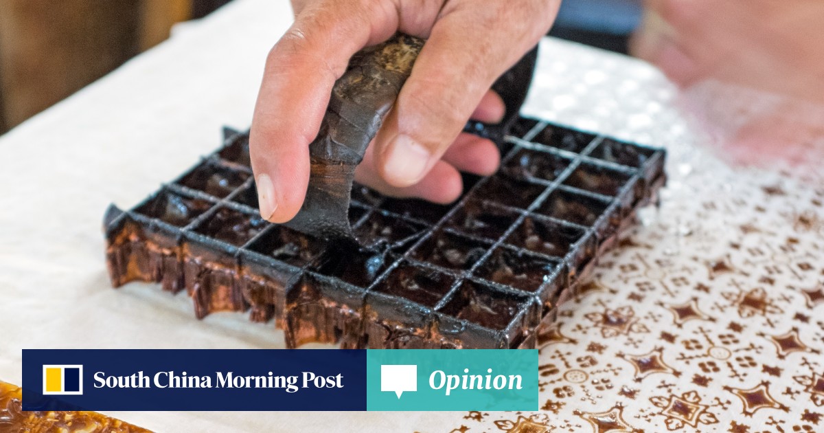
Throughout East Asia, South Asia and Southeast Asia, batik and ikat textiles are produced by weaving together horizontal and vertical lines of cotton or silk thread in a loom, and then dyeing the threads with different colours. In the batik process, the cloth is covered with wax, and the pattern is printed through a hot copper design block that melts the wax beneath.
When the cloth is then put into a vat of dye, only those parts where the wax has melted would be dyed. The process is repeated with different designs and dyes.
The same passion that produced the best batik or ikat textiles for centuries is producing the best semiconductor chips today. India, Central Asia and the Middle East all share the same textile traditions, so their potential in chip production cannot be underestimated.
It does not matter whether the best integrated circuit designs are from the United States; that such designs can be engineered in Asia is testimony to long traditions of dedicated craftsmanship.
Huawei’s chip triumph is proof that US tech war on China is sheer folly
Huawei’s chip triumph is proof that US tech war on China is sheer folly
All these suggest that the global supply chain of design, fabrication, fabless and outsourced semiconductor assembly and testing (OSAT) models will not decouple due to geopolitical sanctions or measures. They will simply evolve, innovate and adapt to changing demands.
As Miller brilliantly summed up in Chip War, semiconductor chips have military uses, but their explosion into daily lives came about through the consumer market.
You can restrict the intellectual property rights to 1- or 2-nanometre chips, but the number of such chips necessary to power the latest missiles or drones is small, whereas big numbers of 14nm or 28nm chips are needed for electric vehicles and digital home appliances. In the end, the mass producer will always overwhelm the small producer.
Scale is a quality that cannot be ignored. Those who understand history remember that time and opportunity move in cycles. The poor do not stay poor forever. And knowledge cannot be contained or confined to a few. That is why I am increasingly confident that the rest of the world will break out of their tech containment by an increasingly insecure West weaponising everything from artificial intelligence to chips.
Andrew Sheng is a former central banker who writes on global issues from an Asian perspective


